GaN Template Grow Application SSP Sapphire Carrier Substrate Chip
1. What is templates
We use the term "template" to describe our products as they are different to substrates. Specifically, a template is a composite or engineered substrate, where one or more layers are added to the original susbstrate.
2.Application
Blue and white LED for room lightings, displays and general use
GaN power switching devices
3.Product available
2" to 4" GaN-templates on FSS and PSS
Thick GaN-templates (t=3~20μm)
GaN-template with highly doped n-type layer (n=<1e19/cm3)
Ntype (undoped), Ntype (Si doped), and Ptype(Mg doped) templates are available
GaN Templates on both sapphire substres and Silicon substrates
4. Features
| XRD-FWHM | 002 | 102 |
| 3-4μm GaN/Sapphire | 200-300 | 250-450 |
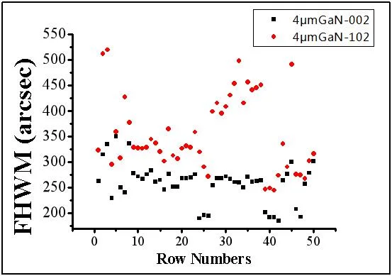
Dislocation density:3.5E+08 cm-2
5. Specification
2inch specification
| Item | GaN-FS-C-U-C50 | GaN-FS-C-N-C50 | GaN-FS-C-SI-C50 |
| Dimensions | Ф 50.8 mm ± 1 mm | ||
| Thickness | 350 ± 25 µm | ||
| Useable Surface Area | > 90% | ||
| Orientation | C-plane (0001) off angle toward M-Axis 0.35°± 0.15° | ||
| Orientation Flat | (1-100) ± 0.5°, 16.0 ± 1.0 mm | ||
| Secondary Orientation Flat | (11-20) ± 3°, 8.0 ± 1.0 mm | ||
| Total Thickness Variation | ≤ 15 µm | ||
| BOW | ≤ 20 µm | ||
| Conduction Type | N-type (Undoped) | N-type (Ge-doped) | Semi-Insulating (Fe-doped) |
| Resistivity(300K) | < 0.5 Ω·cm | < 0.05 Ω·cm | >106 Ω·cm |
| Dislocation Density | 1~9x105 cm-2 | 5x105 cm-2 ~3x106 cm-2 | 1~9x105 cm-2 |
| 1~3x106 cm-2 | 1~3x106 cm-2 | ||
| Polishing | Front Surface: Ra < 0.2 nm. Epi-ready polished Back Surface: Fine ground | ||
| Package | Packaged in a class 100 clean room environment, in single wafer containers, under a nitrogen atmosphere. | ||
4inch specification
| Item | GaN-T-C-U-C100 | GaN-T-C-N-C100 |
| Dimensions | Ф 100 mm ± 0.1 mm | |
| Thickness | 4 µm, 20 µm | |
| Orientation | C-plane(0001) ± 0.5° | |
| Conduction Type | N-type (Undoped) | N-type (Si-doped) |
| Resistivity 300K | < 0.5 Ω·cm | < 0.05 Ω·cm |
| Carrier Concentration | < 5x1017 cm-3 | > 1x1018 cm-3 |
| Mobility | ~ 300cm2/V·s | ~ 200 cm2/V·s |
| Dislocation Density | Less than 5x108 cm-2 | |
| Substrate structure | GaN on Sapphire(Standard: SSP Option: DSP) | |
| Useable Surface Area | > 90% | |
| Package | Packaged in a class 100 clean room environment, in cassettes of 25pcs or single wafer containers, under a nitrogen atmosphere. | |
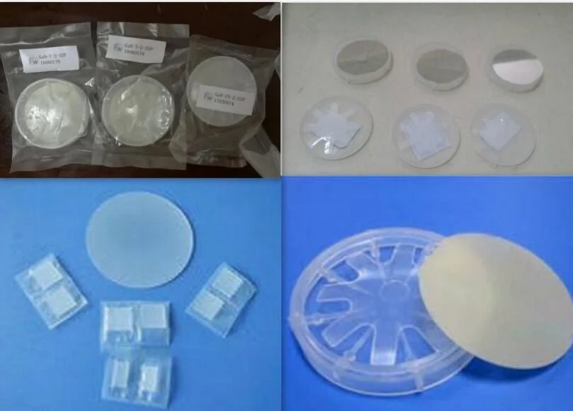
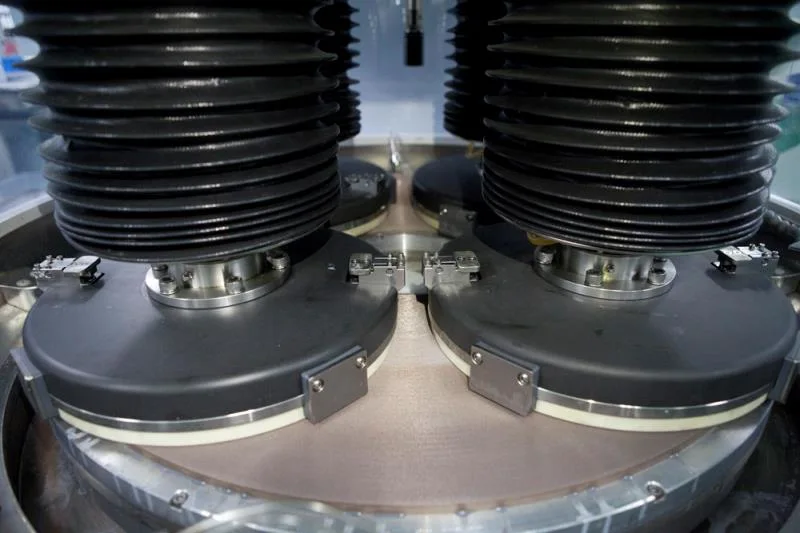
6. Product pictures